M8: a CPU built from logic blocks
An 8-bit accumulator processor with a gate-based ALU, program counter, instruction ROM, data RAM, branches and seven-segment display drivers.
Hardware simulation result
The ROM program computes 1 + 2 + 3 + 4 + 5 using a countdown loop. The RTL reaches HALT after 54 instructions and latches decimal 15 to the output register.
This viewer replays signal values recorded by the Verilog testbench. It is not a connection to a physical FPGA.
Gate-level architecture
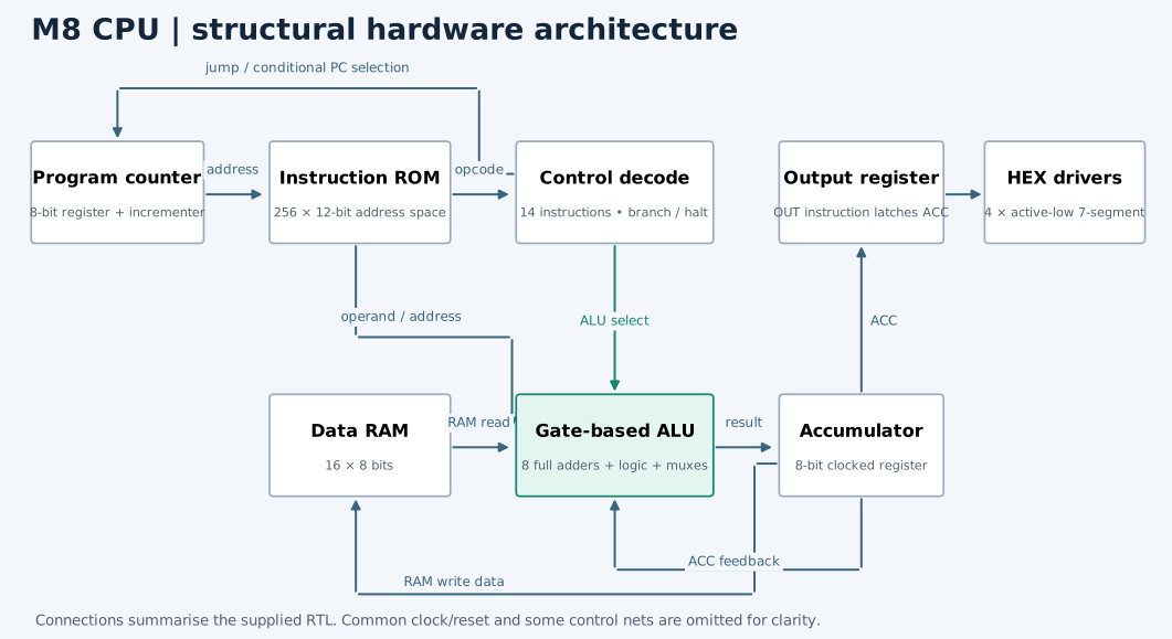
Eight full-adder cells form the ripple-carry arithmetic unit. XOR gates select subtraction; gate-based multiplexers select the result.
Single-clock execution with enable signals, conditional branching, a latched output, halt control and invalid-instruction faults.
Synchronized controls, a debounced step button and four active-low seven-segment buses. Exact device and pins remain unset.
Recorded execution trace
| Cycle | Next PC | Accumulator | RAM[0] | RAM[1] | Output | HALT |
|---|
Waveforms from the hardware simulation
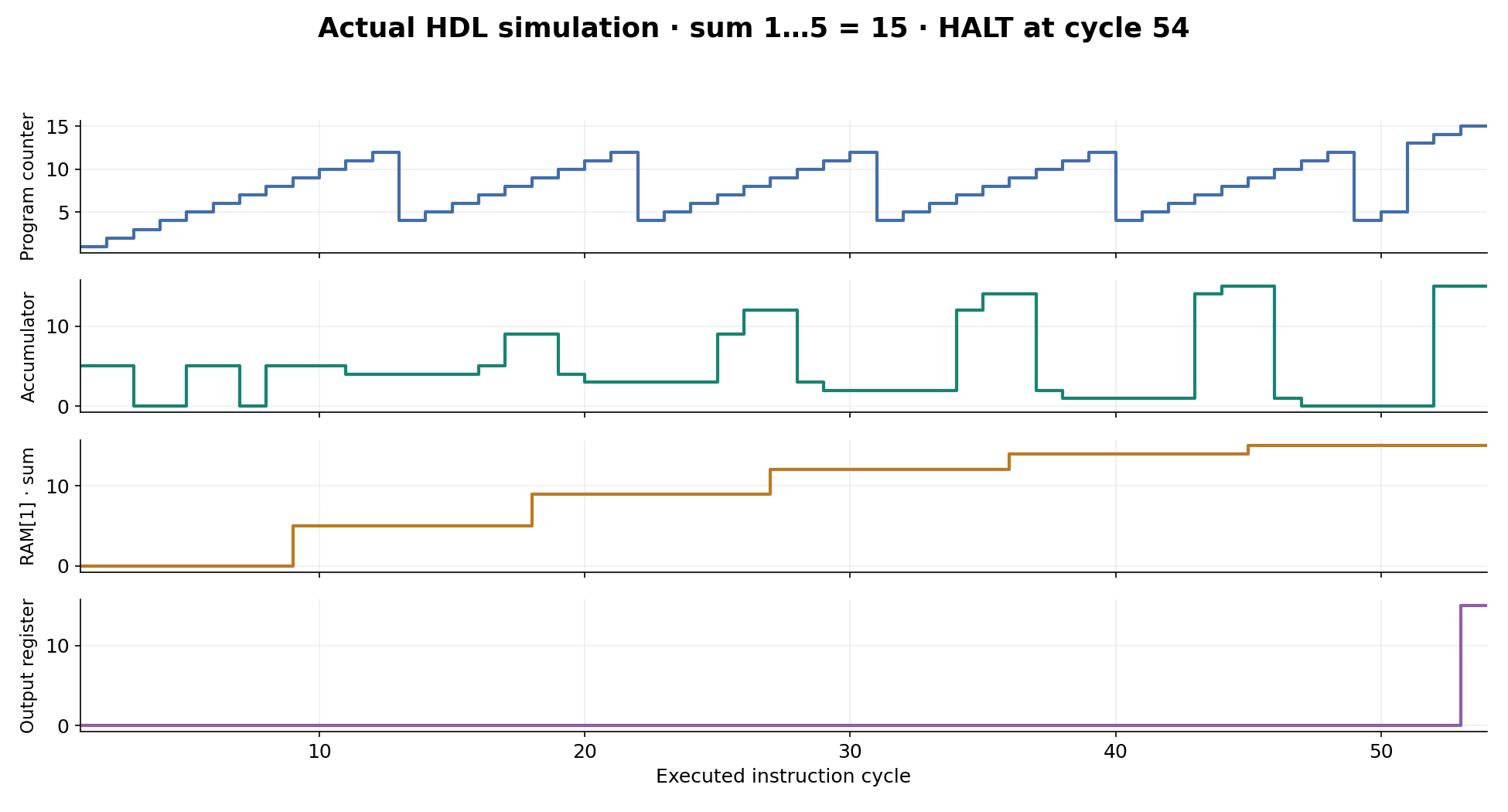
The plot uses the testbench’s recorded signals. The downloadable VCD contains the underlying clock, control, register and gate-level transitions.
Inside the arithmetic block
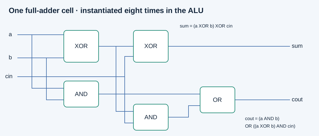
The supplied full_adder module implements these gates directly. Cells are grouped into the ripple-adder block and instantiated in the ALU and program-counter incrementer.
Verification & implementation files
131,072 add/sub input cases and 1,024 bitwise cases passed in the logic simulator.
All 14 instructions, both branch outcomes, RAM bounds, output latching and halt behaviour passed.
The simulated board interface passed stepping and run-control tests. Final output segment codes decode to 0F.
Includes structural RTL, assembler, ROM program, testbenches and Quartus QPF/QSF project files. Compilation and simulation used Icarus Verilog 12.0. Quartus synthesis, fitting, timing closure and programming require the exact board model and a local Quartus installation.